Notes from Ben Eater’s youtube series on building an 8-bit computer.
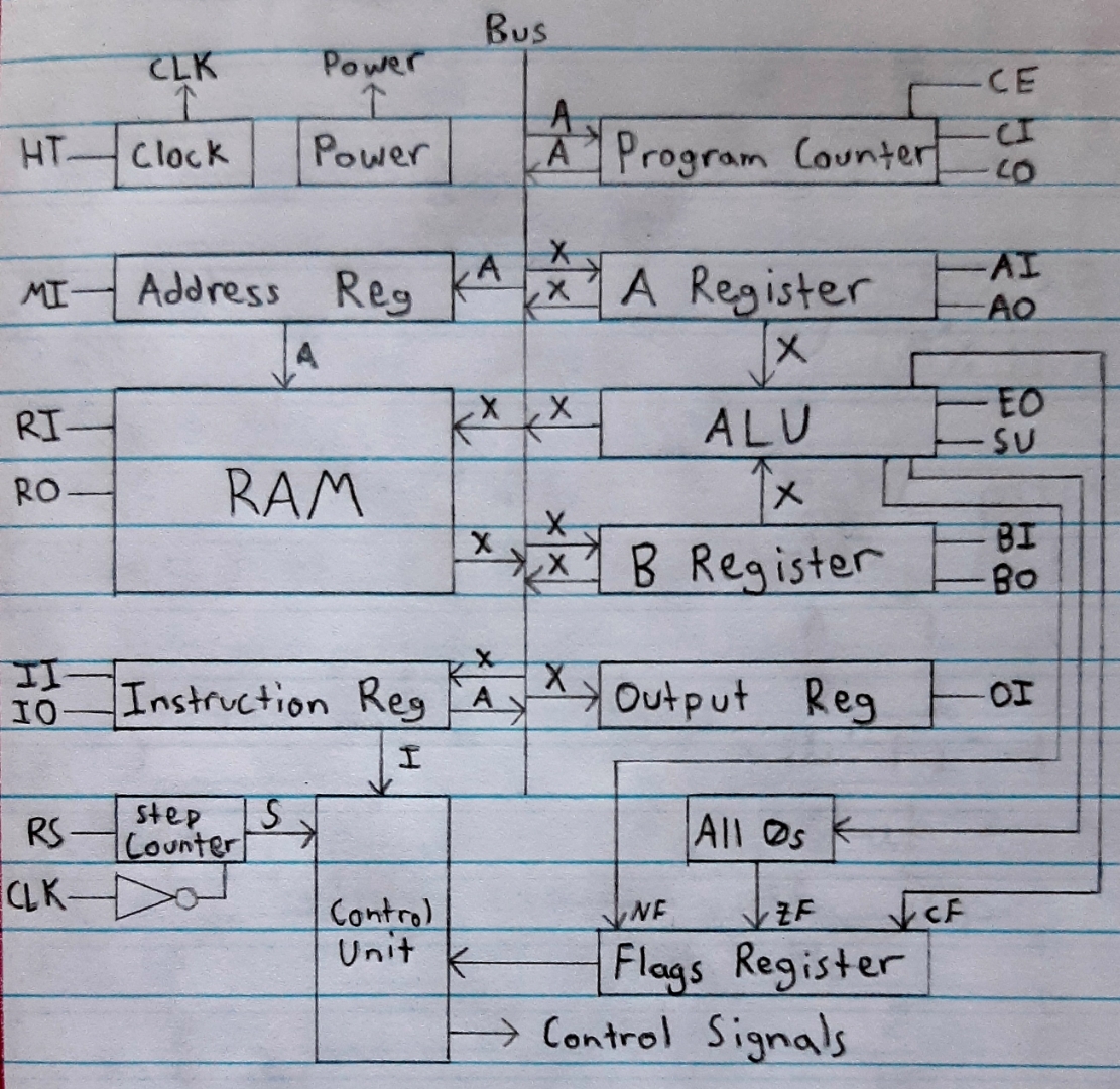
Xs on any diagram represent the amount of connections equal to the base of the computer.
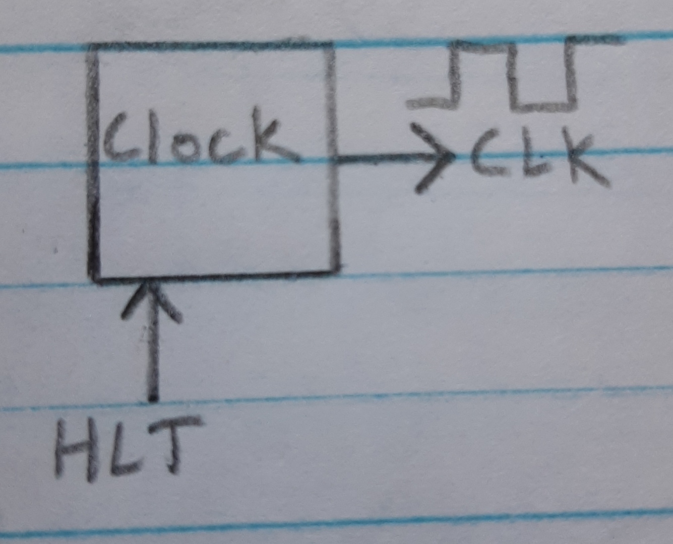
The clock signal is like the heart beat of the computer. It is a repeating pattern of high and low voltage which is used across the CPU in order to sync the execution of different components.

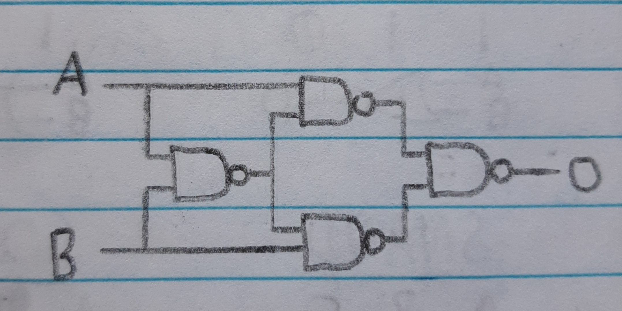
Logic gates are used to perform the logic within the computer. Modules are constructed from many of these logic gates in order to perform specialized operations.
| Common gates | 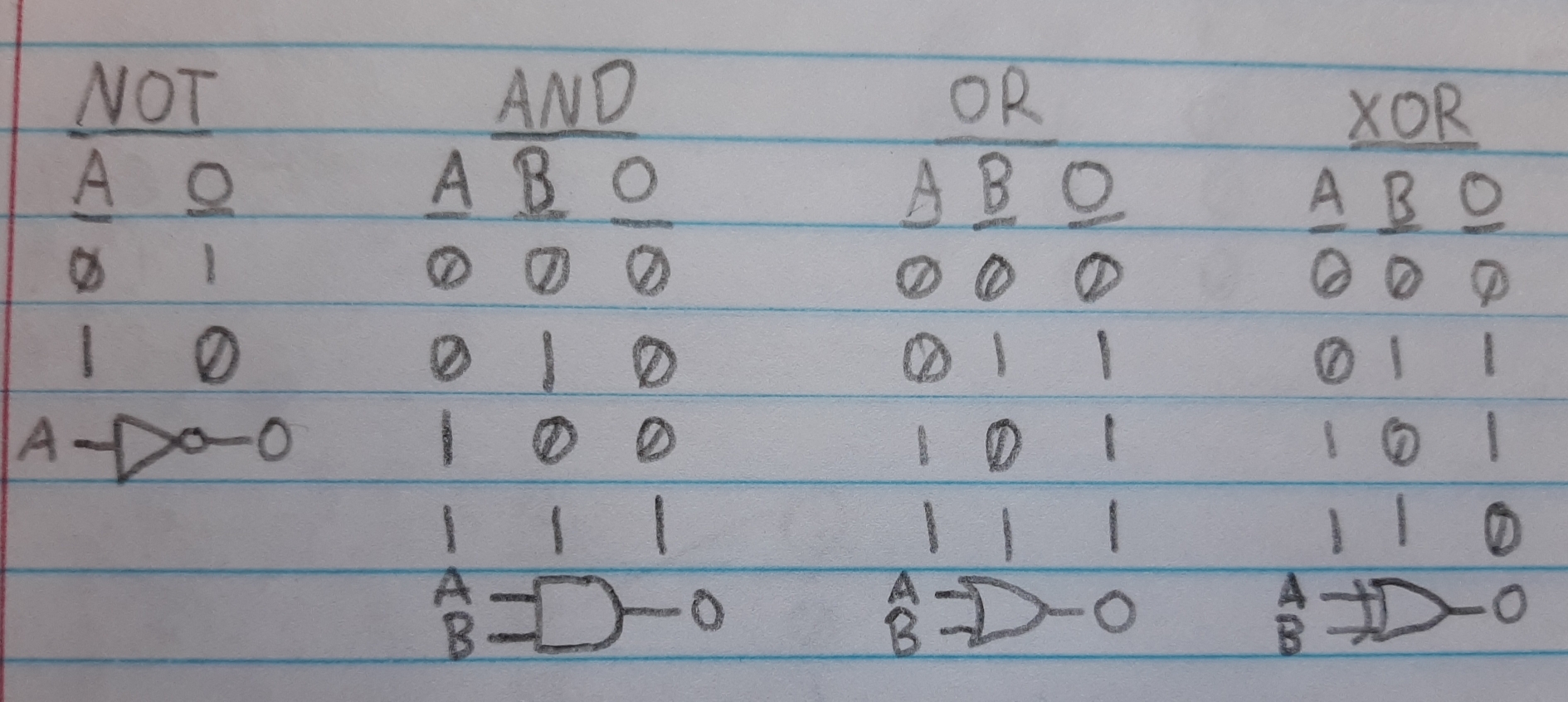 |
| Inverse gates | 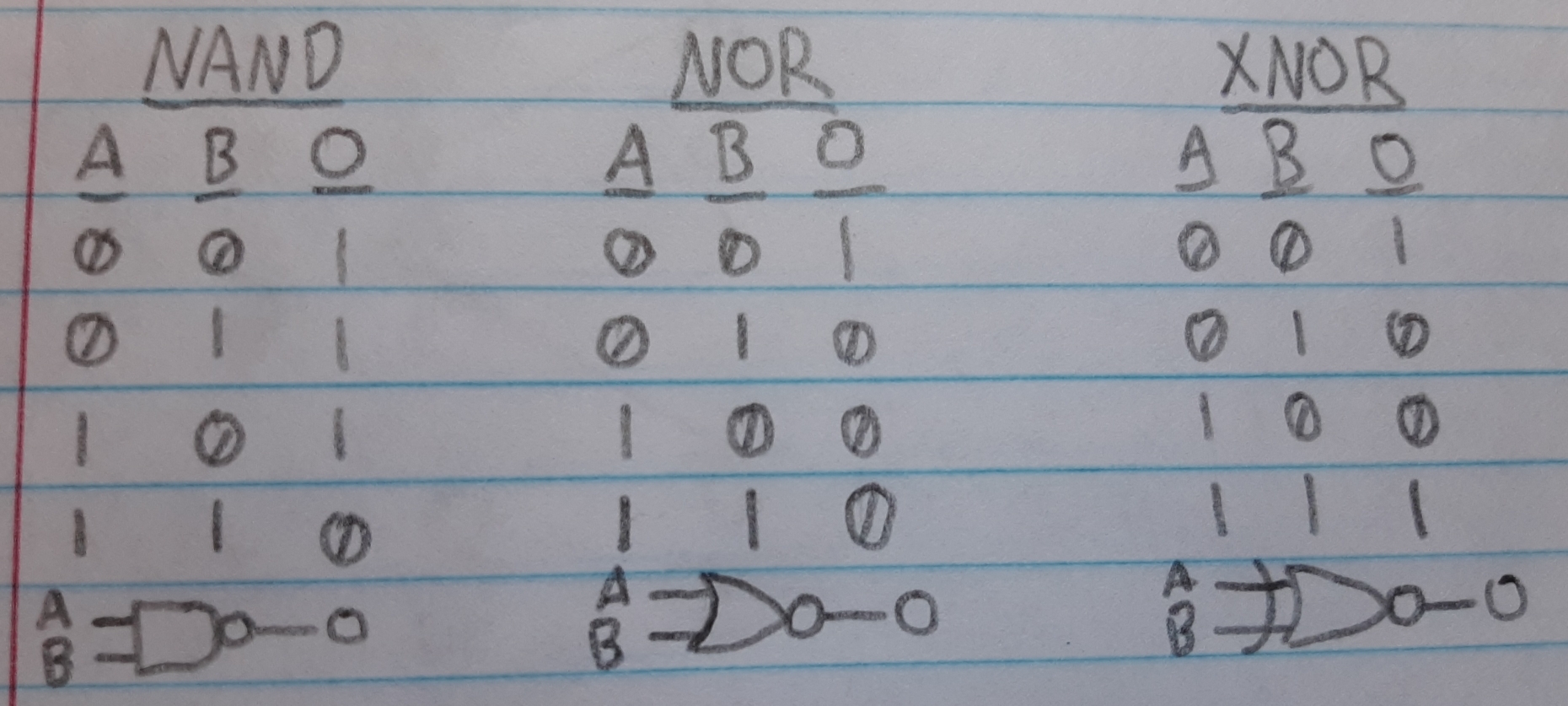 |
| Selective input gates | 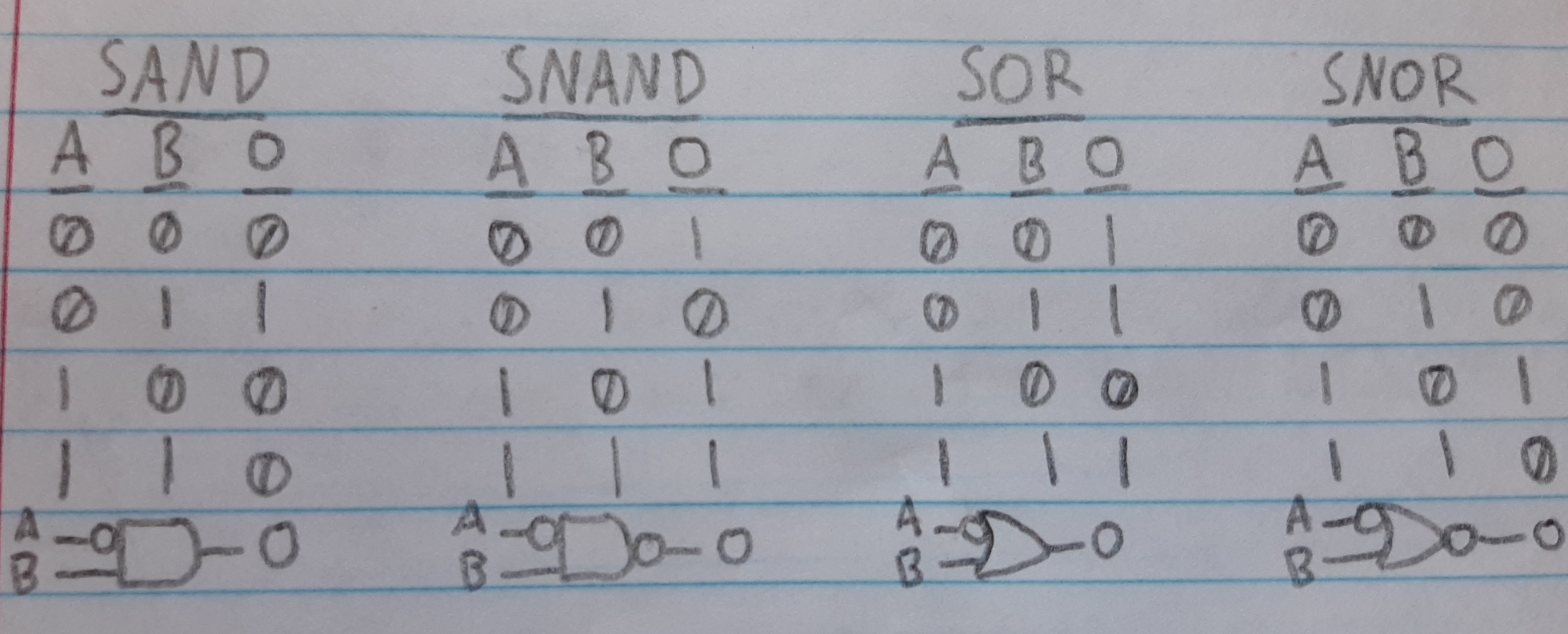 |
Logic gates can be created from transitions/digital switches. The most commonly used transistors are MOSFETS.
| NMOS(1 On and 0 Off) | 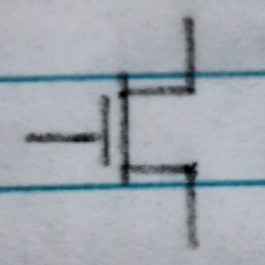 |
PMOS(0 On and 1 Off) | 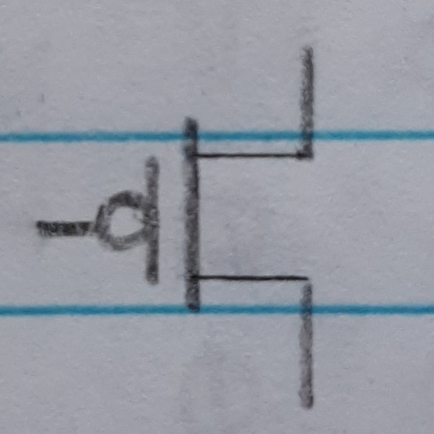 |
| NOT | 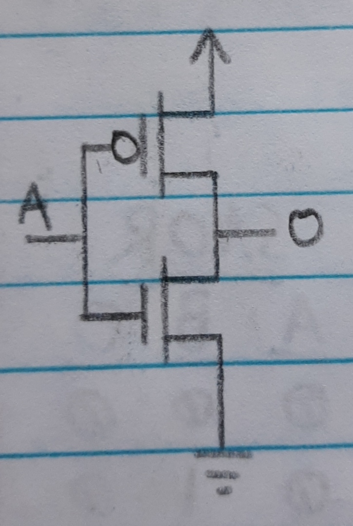 |
NAND | 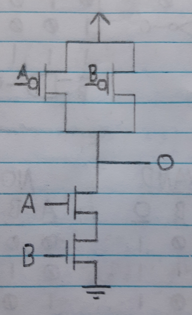 |
NOR | 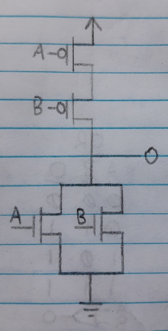 |
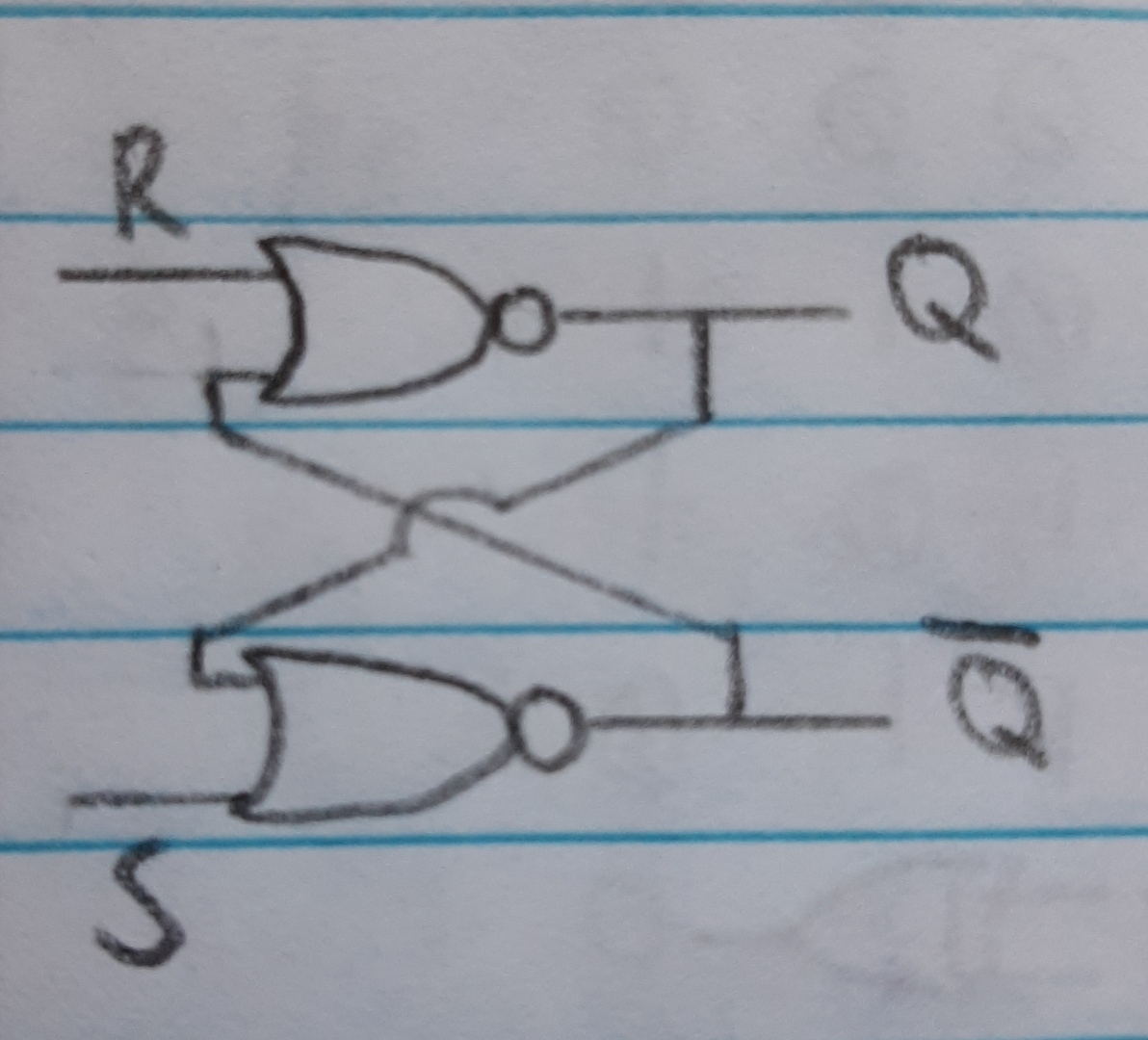
Once the SR Latch is set to 1 or 0 it maintains its state, unlike logic gates.
| S | R | Q | !Q |
|---|---|---|---|
| 0 | 0 | Q | !Q |
| 0 | 1 | 0 | 1 |
| 1 | 0 | 1 | 0 |
| 1 | 1 | Unknown | Unknown |
 |
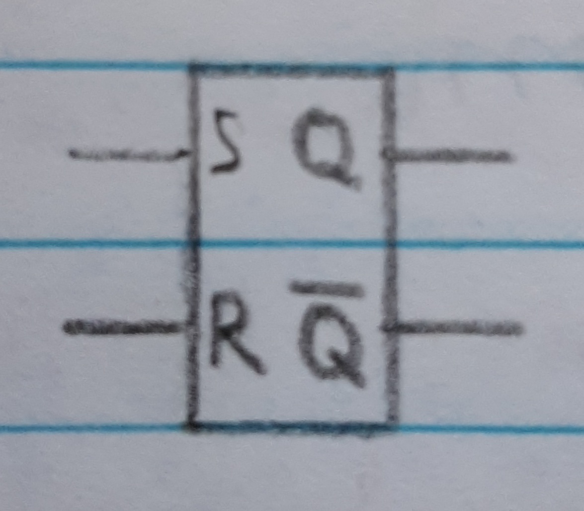 |
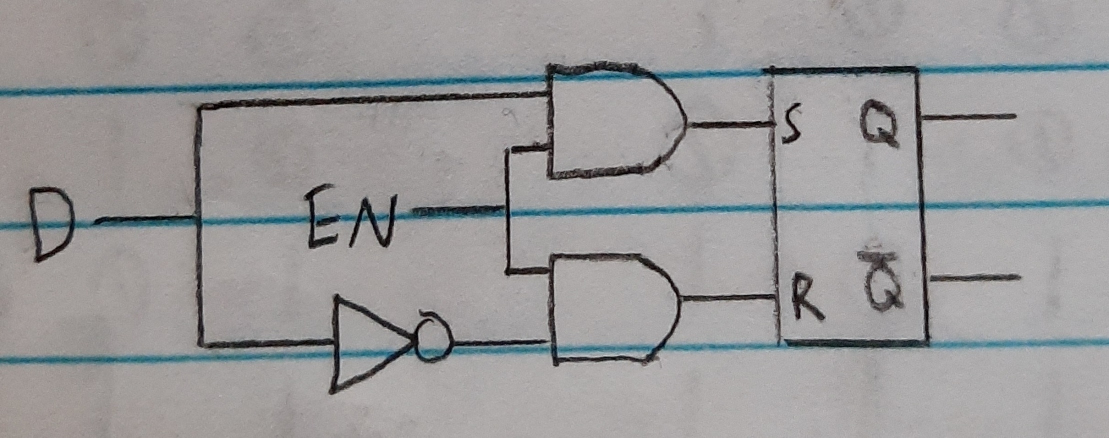
The D latch is a modification to the SR latch to allow for one input(D) to set and reset it. This input(D) only works when the enable pin(EN) is set.
| EN | D | Q | !Q |
|---|---|---|---|
| 0 | 0/1 | Q | !Q |
| 1 | 0 | 0 | 1 |
| 1 | 1 | 1 | 0 |
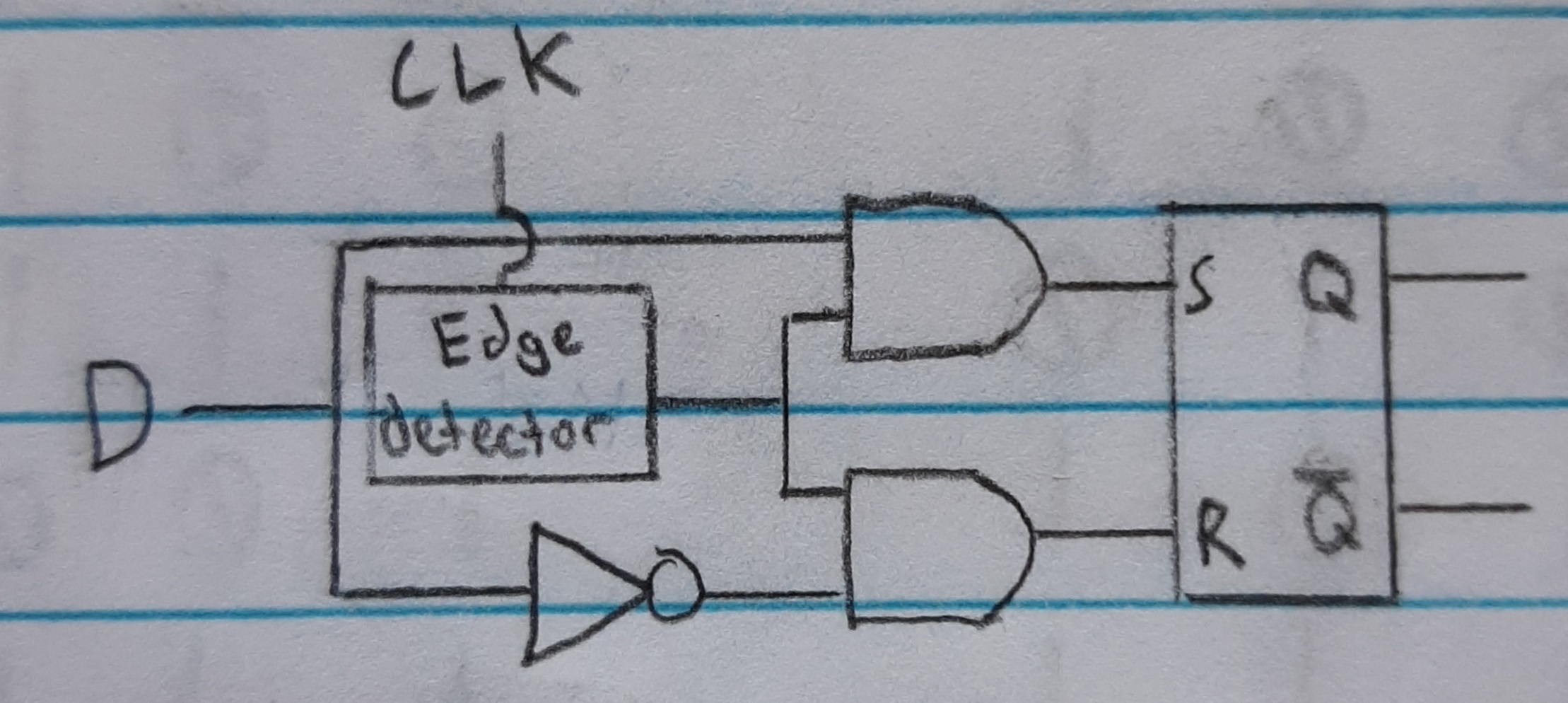
The D Flip-Flop is like the D Latch, but only activates when the clock signal goes from low to high.
 |
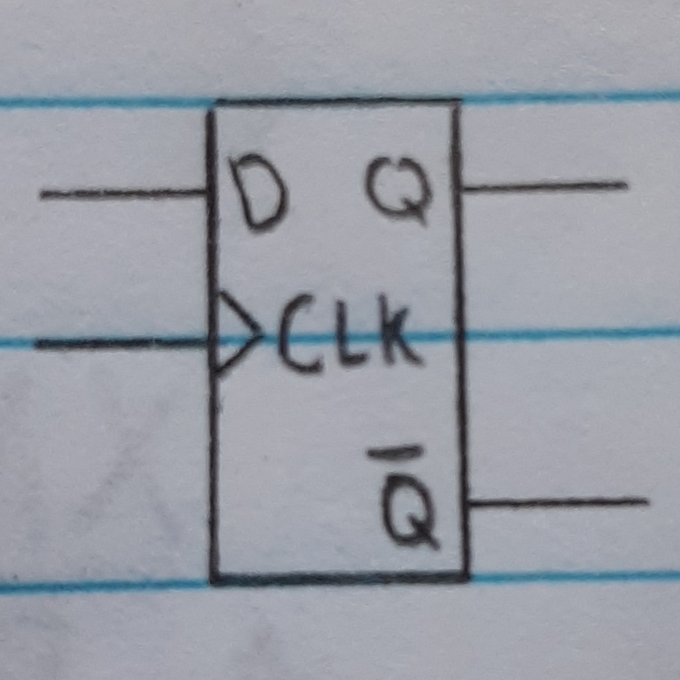 |
| CLK | D | Q | !Q |
|---|---|---|---|
| X | 0/1 | Q | !Q |
| 0 to 1 | 0 | 0 | 1 |
| 0 to 1 | 1 | 1 | 0 |
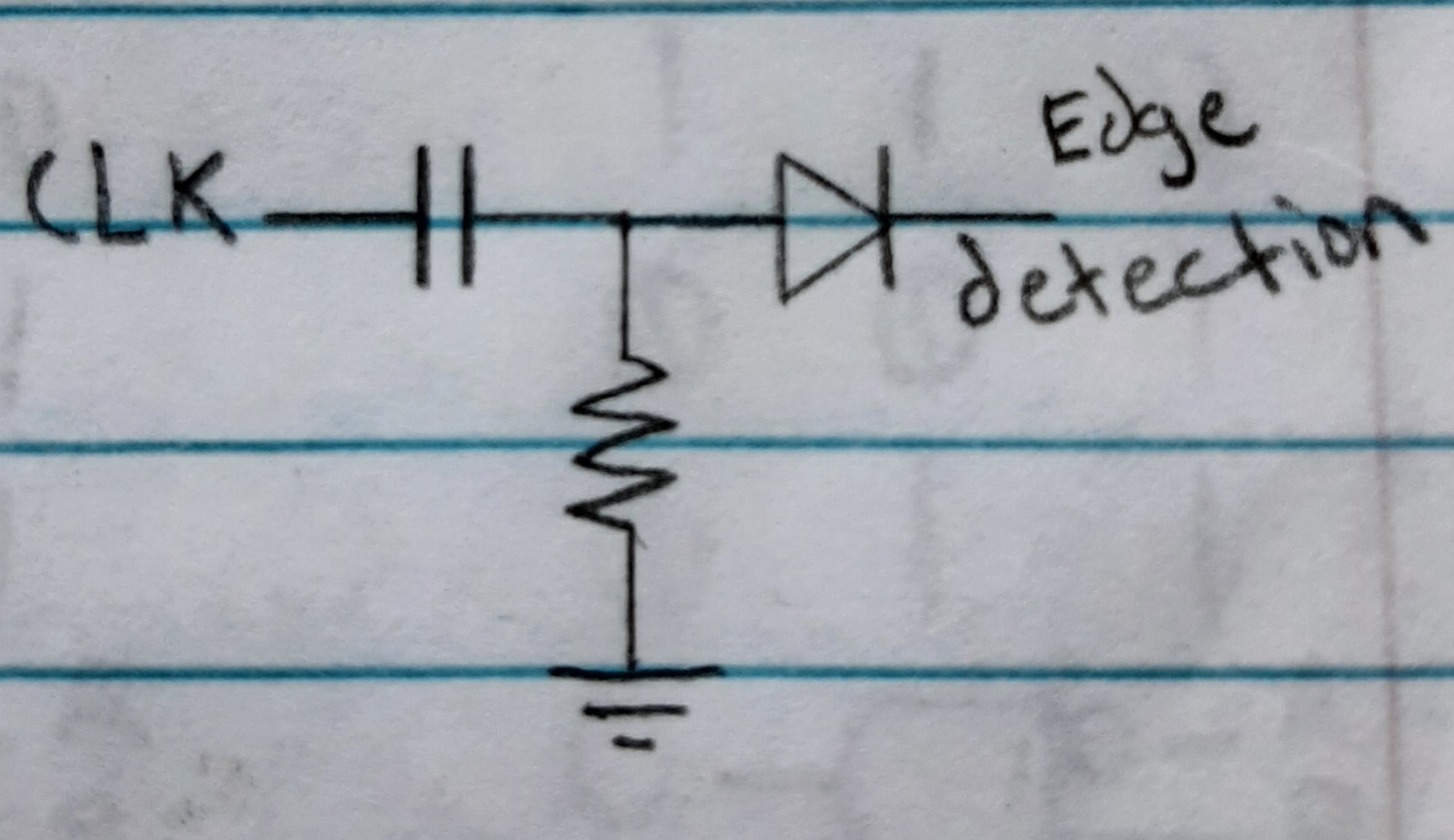
In order to detect when the clock goes from low to high, you need an edge detection circuit.


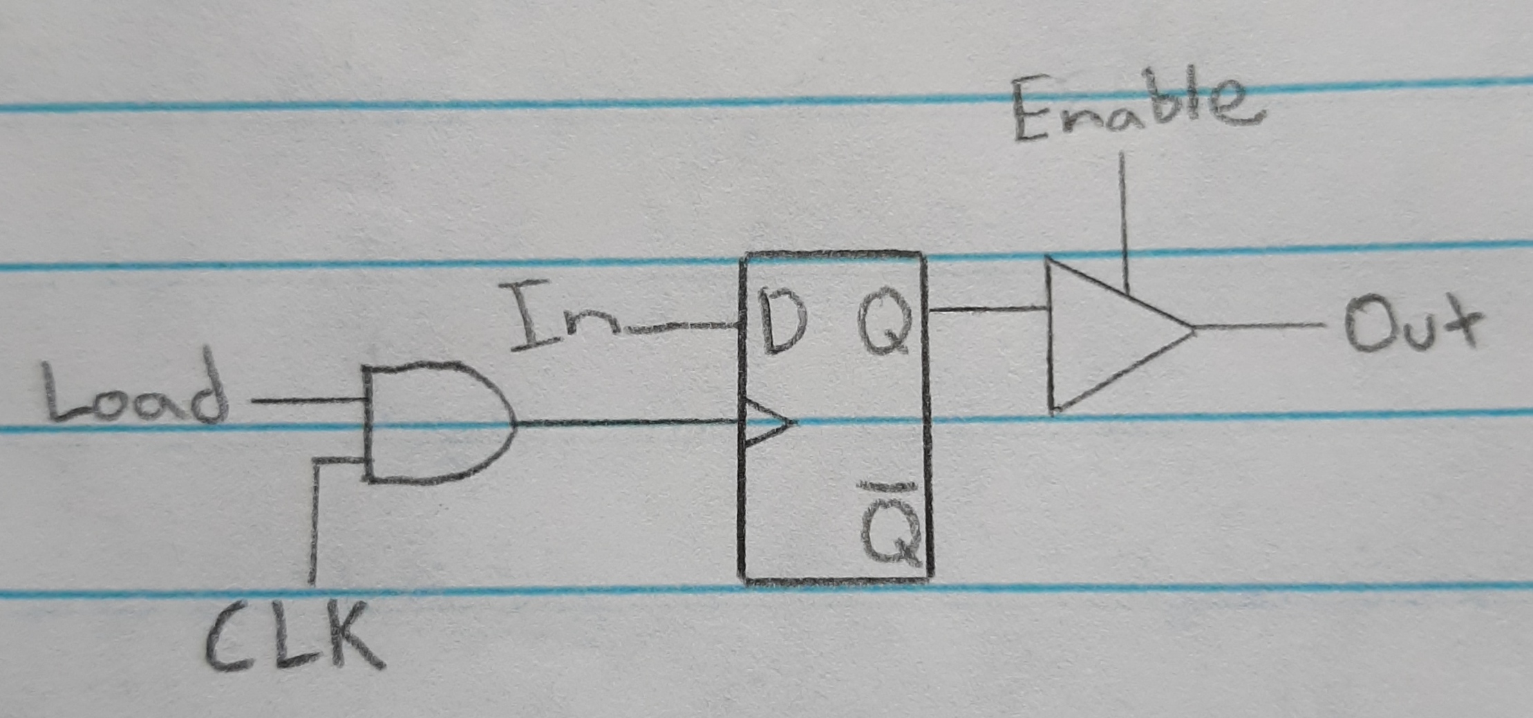
A bus is used for communication between different modules of a CPU. It is a collection of wires, usually the same number as the base of the computer, which connects to all other modules.
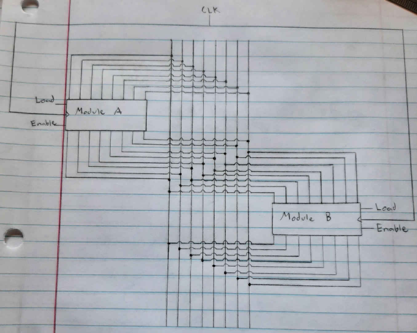
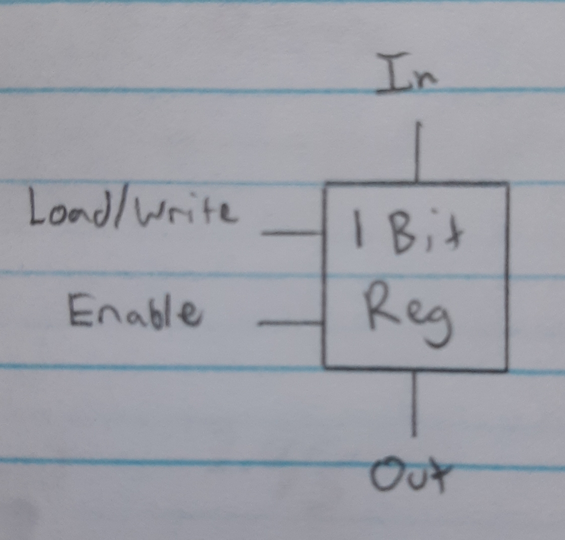
| Enable | Load | Description |
|---|---|---|
| 0 | 0 | Neither/Floating |
| 1 | 0 | Put data onto the bus |
| 0 | 1 | Read data from the bus |
| 1 | 1 | Never used |
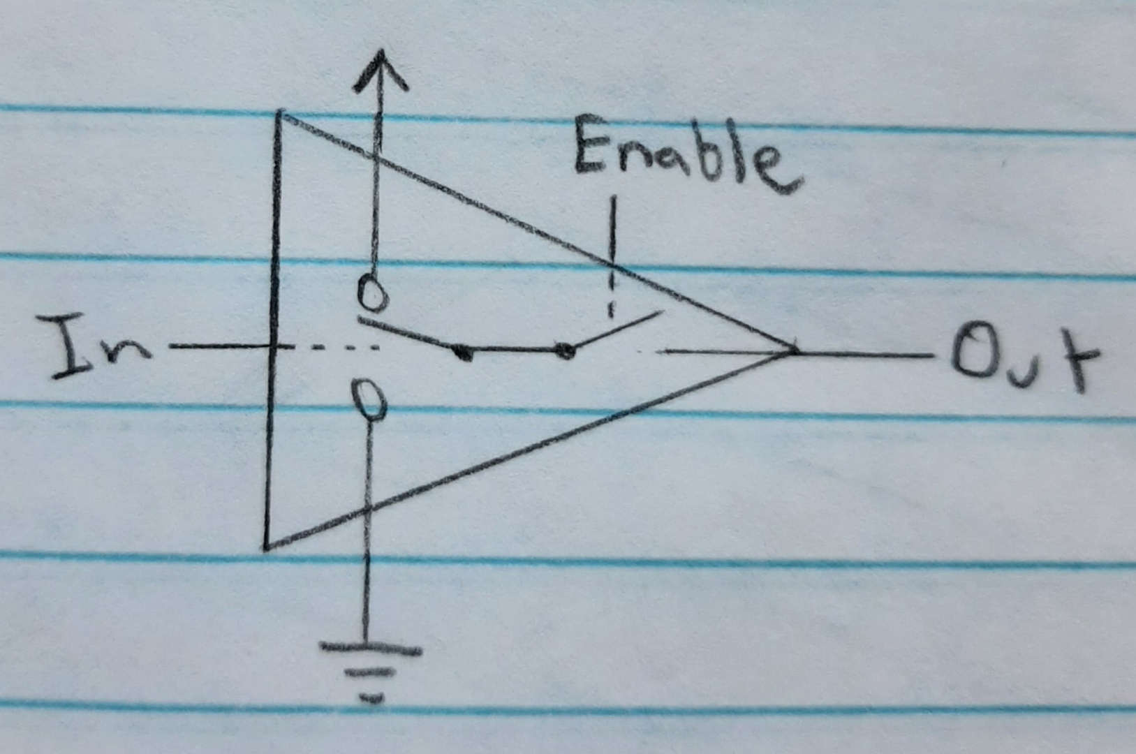
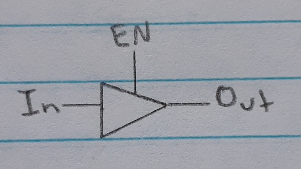
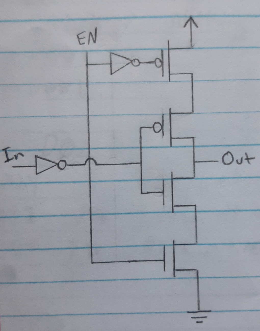
In order to have a floating output(not set to 1 or 0) you need to decouple it from the bus.
| In | En | Out |
|---|---|---|
| 0 | 0 | Hi-Z/Floating |
| 1 | 0 | Hi-Z/Floating |
| 0 | 1 | 0 |
| 1 | 1 | 1 |
 |
 |
 |
A register is a module that is used to store a word, same bits as the computer base, of memory inside the CPU.
 |
 |
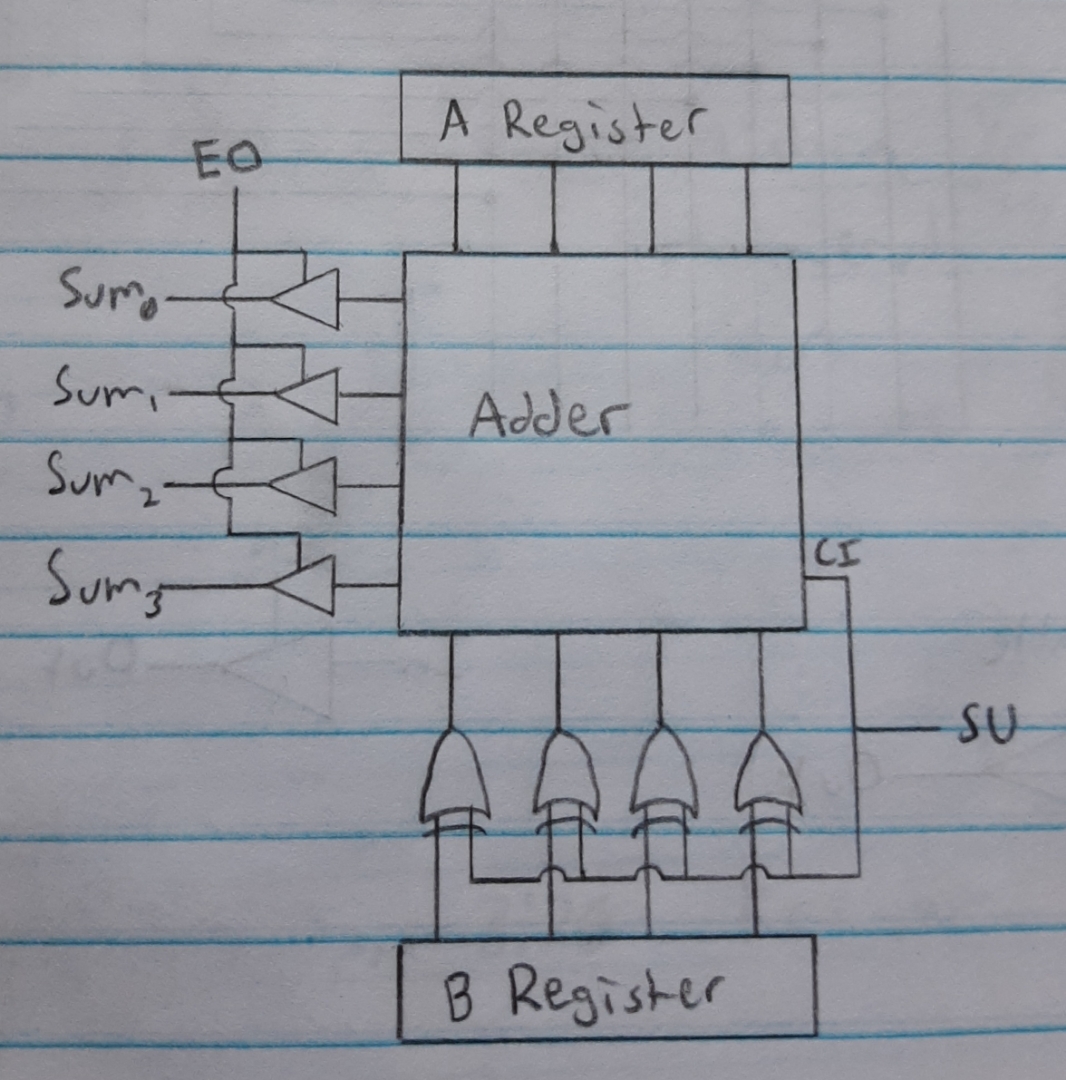
The arithmetic logic unit (ALU) is the module in the CPU which does mathematical and logical operations. It is connected to registers and can transfer the results to the bus.
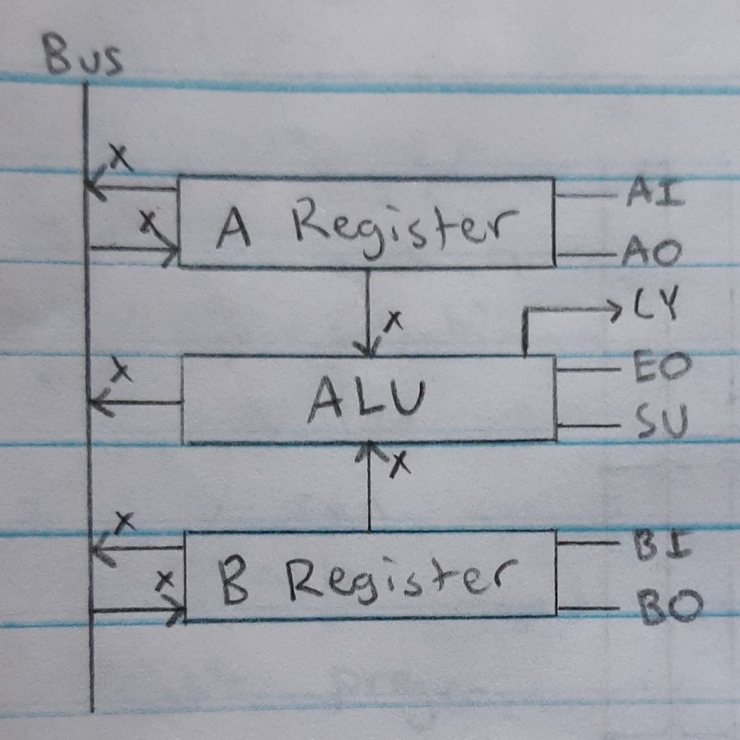
X symbolizes the amount of connections equal to the base of the computer.| Control Signal | Description |
|---|---|
| AI | A register In/Load |
| AO | A register Out/Enable |
| CY | Carry Bit |
| EO | Sum Out/Enable |
| SU | Subtract |
| BI | B register In/Load |
| BO | B register Out/Enable |
Twos complement is a protocol for converting binary numbers to base 10 numbers. This protocol allows for binary addition and subtraction to translate into base 10 addition and subtraction.
| Binary | Base 10 | Binary | Base 10 |
|---|---|---|---|
| 1000 | -8 | 0000 | 0 |
| 1001 | -7 | 0001 | 1 |
| 1010 | -6 | 0010 | 2 |
| 1011 | -5 | 0011 | 3 |
| 1100 | -4 | 0100 | 4 |
| 1101 | -3 | 0101 | 5 |
| 1110 | -2 | 0110 | 6 |
| 1111 | -1 | 0111 | 7 |
  -5  ->   1011
+  5  -> + 0101
-----    -------
   0  <-  10000

  -7  ->   1001
+  2  -> + 0010
-----    -------
  -5  <-   1011
To convert a number between negative and positive(and vise versa) in two’s complement, you first invert all the bits and then add 1.
-7  ->  1001   Convert to binary
1001 -> 0110   Invert/Flip bits
0110 -> 0111   Binary Add 1
0111  -> 7     Convert to decimal
A full adder is used to add two bits together. The Carry In(CI) input is used to allow for the inclusion of a carry bit from another addition. The Carry Out(CO) output is set to 1 when the addition results in a carry output and 0 when it’s not.
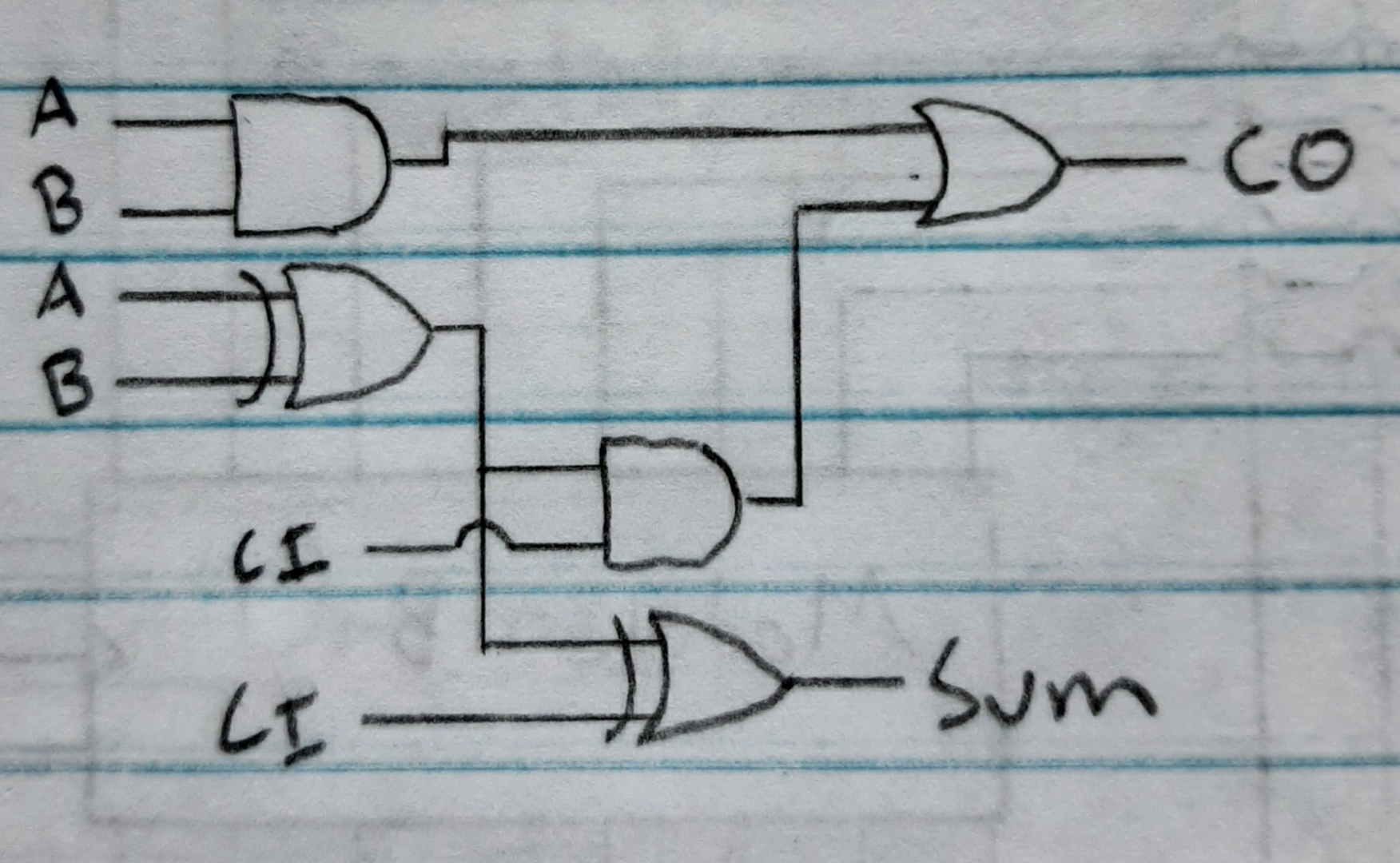 |
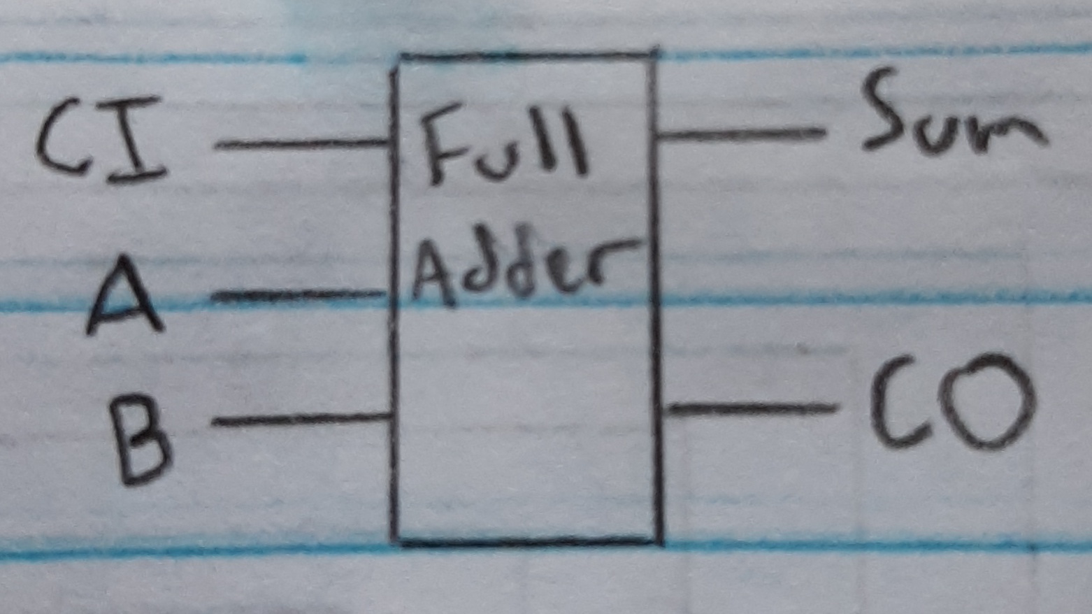 |
Full adders are strung together to do addition on the full word of a computer.
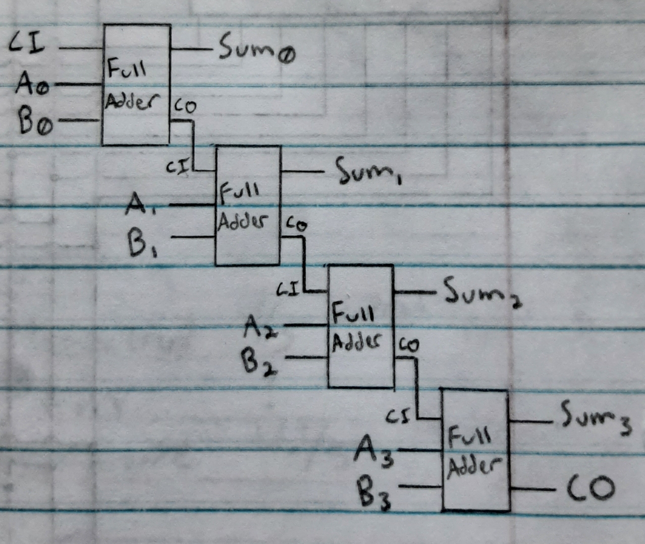
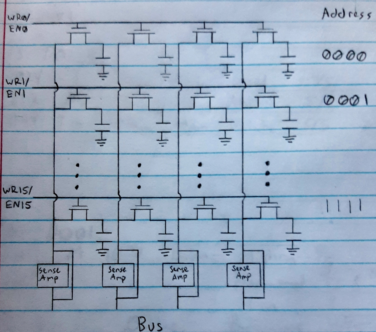
Random Access Memory (RAM) is a sequence of memory locations used to store data, usually the size of a word.
Ex: 4 bit address and 4 bit word memory. The tops and bottoms are connected to the bus with tri-state gates. Separate tri-state gates are used to determine if it should input or output to/from the bus.
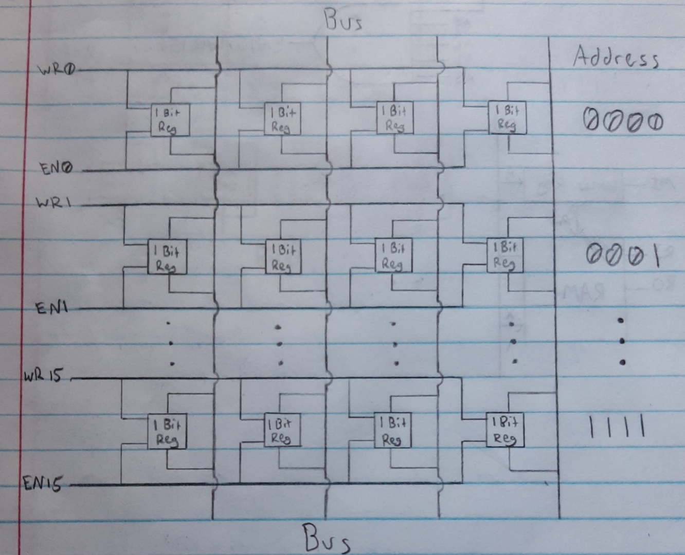
| DRAM | SRAM |
|---|---|
 |
 |
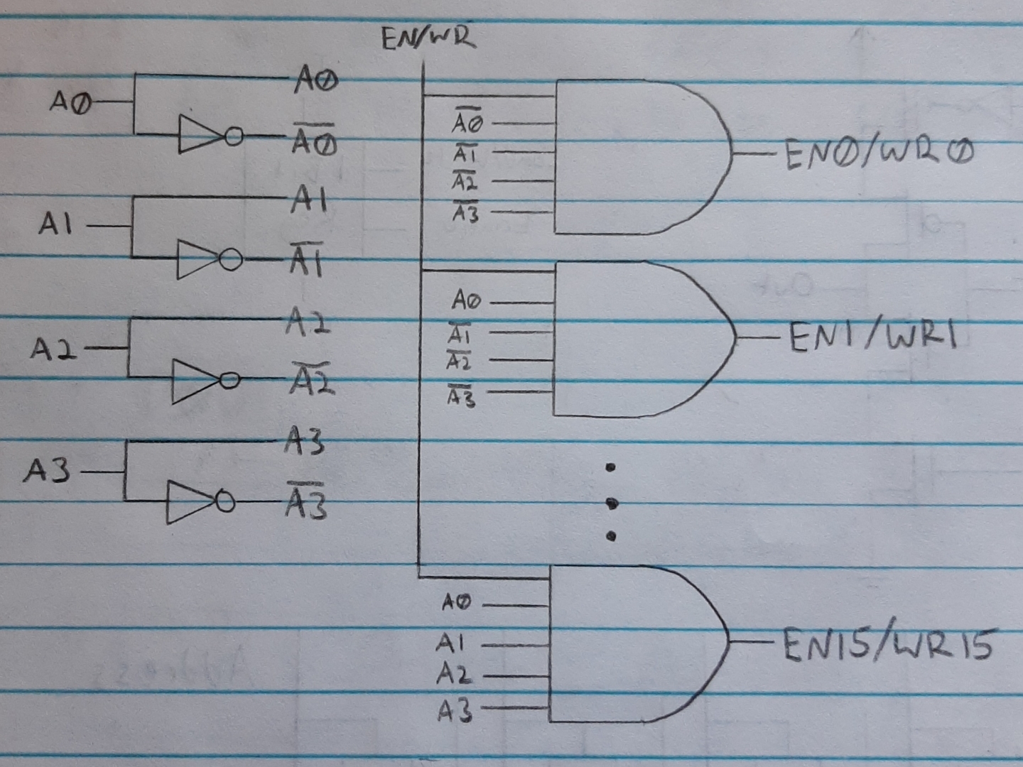
The address mapper/binary decoder is used to map the address to the corresponding WR/EN pins. This can be done with multi-input AND gates.
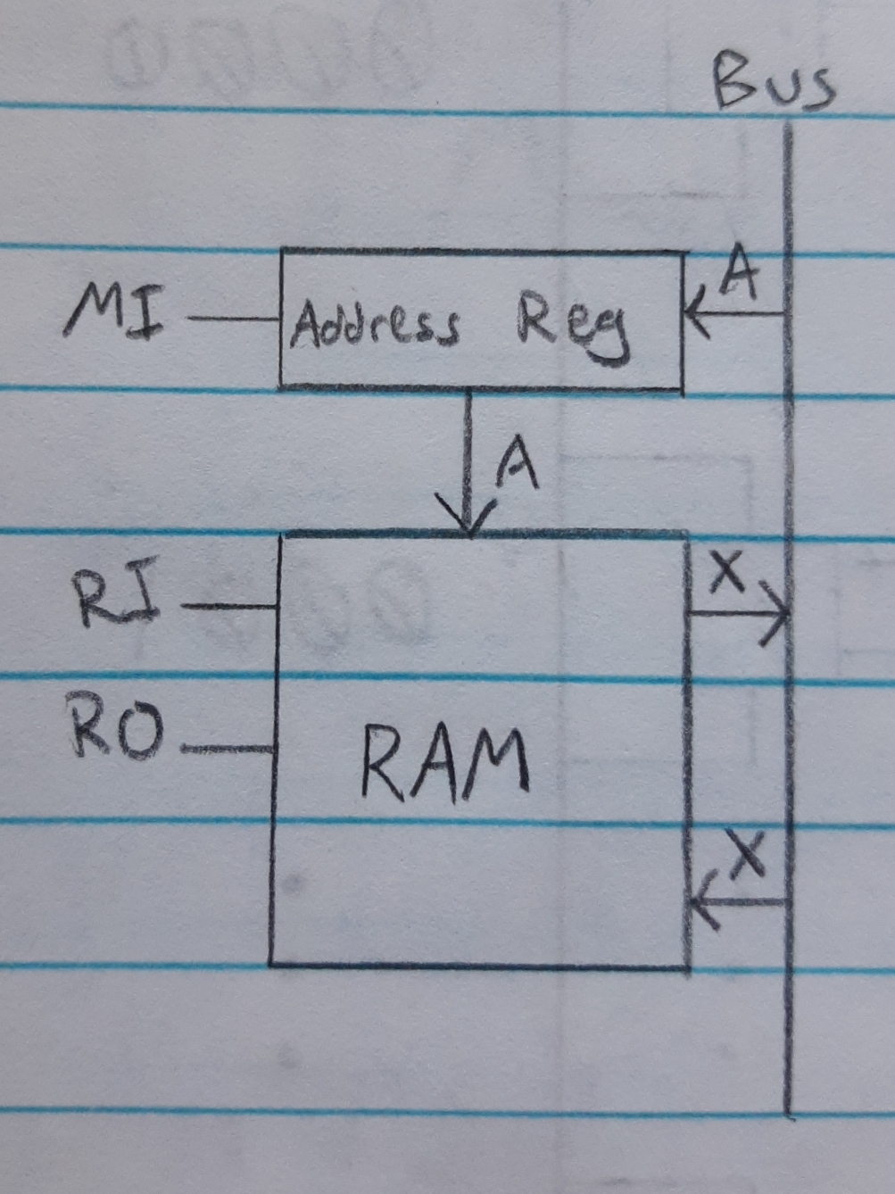
A is the Address size. In this CPU architecture the address size is assumed to be less than the word of the computer to allow one operation to set the address and instruction code.| Control Signal | Description |
|---|---|
| MI | Memory Address In |
| RI | RAM In |
| RO | RAM Out |
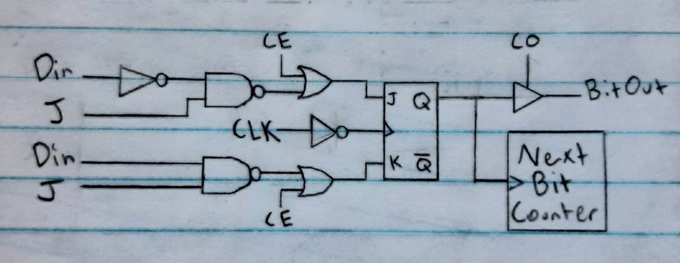
The program counter is used to keep track of which address in RAM is being currently ran.
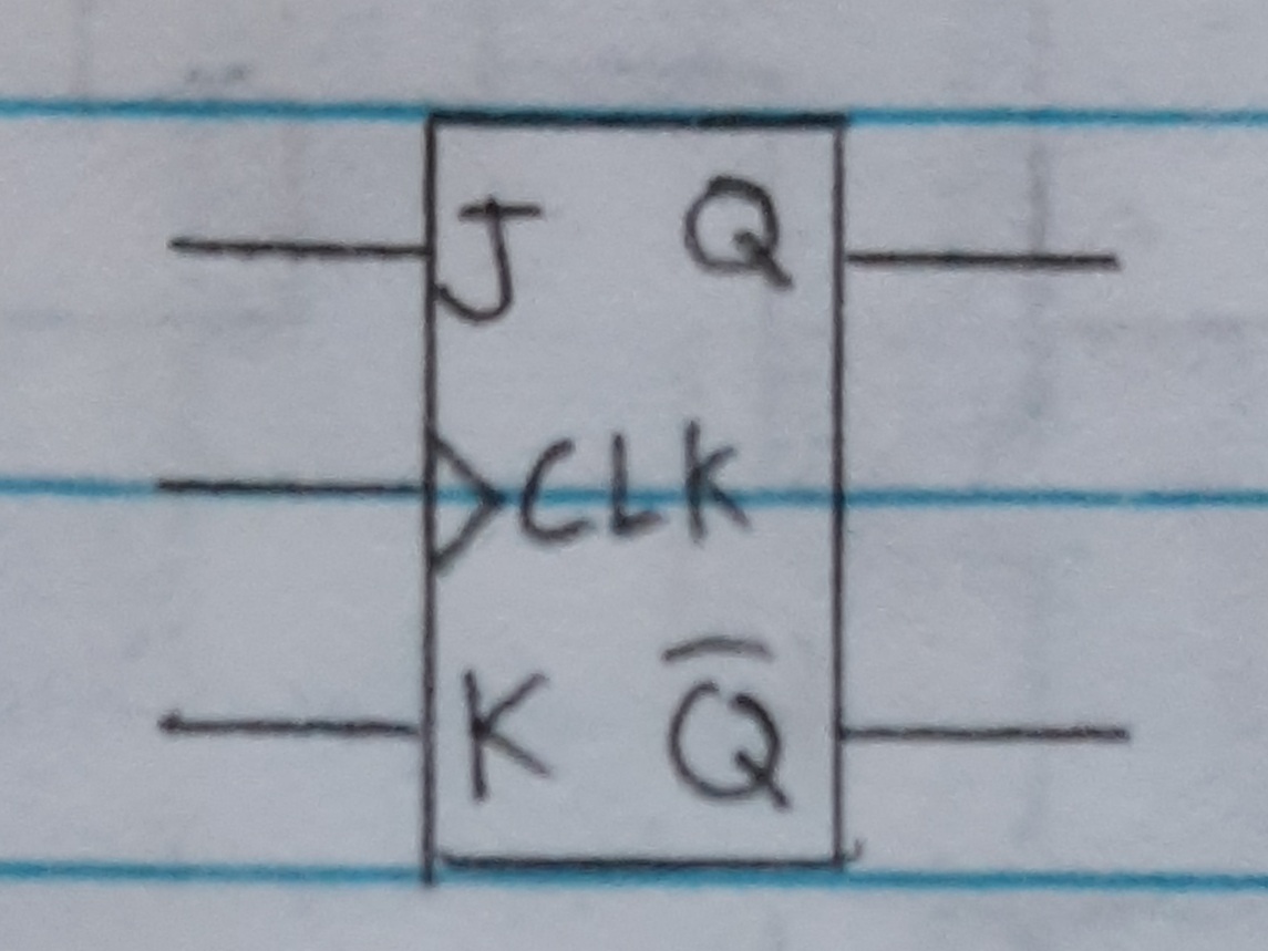
The JK Flip Flop is like the SR Latch, but when both the inputs are high it toggles the state instead of putting it in an unknown state.
| CLK | J | K | Q | !Q |
|---|---|---|---|---|
| X | 0/1 | 0/1 | Q | !Q |
| 0 to 1 | 0 | 0 | Q | !Q |
| 0 to 1 | 0 | 1 | 0 | 1 |
| 0 to 1 | 1 | 0 | 1 | 0 |
| 0 to 1 | 1 | 1 | Toggle | Toggle |
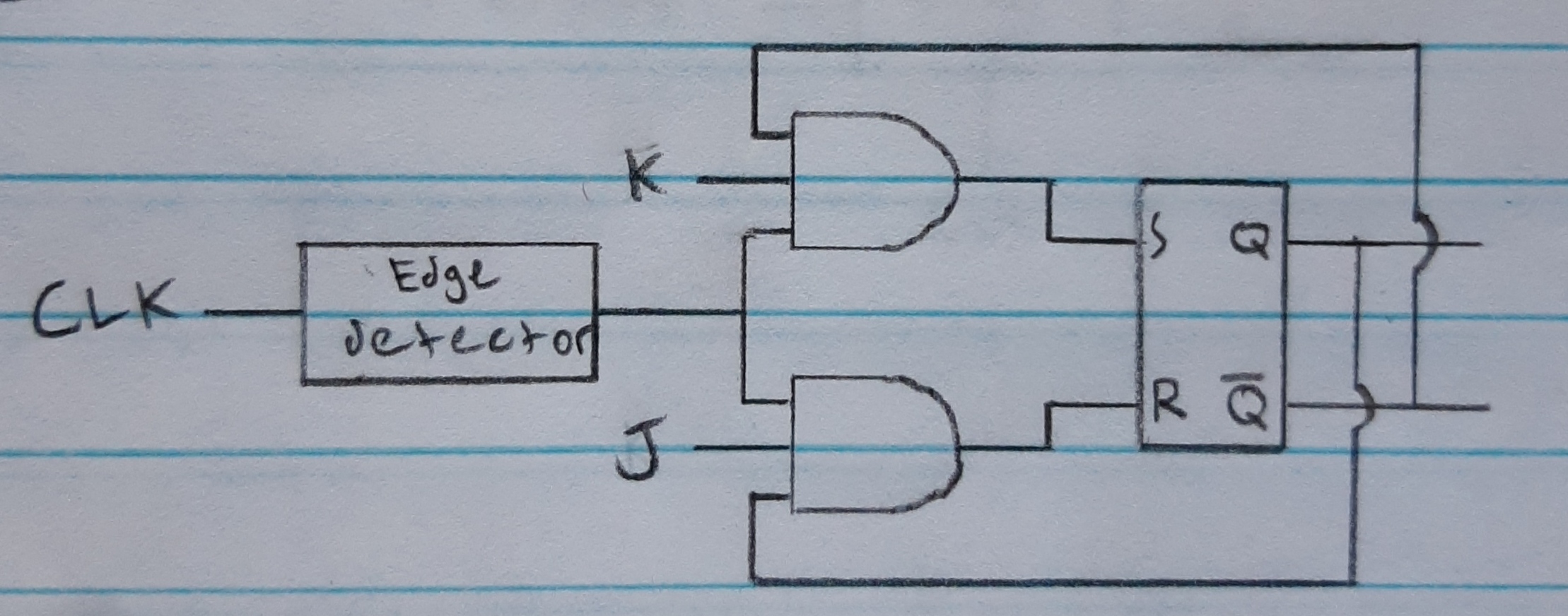
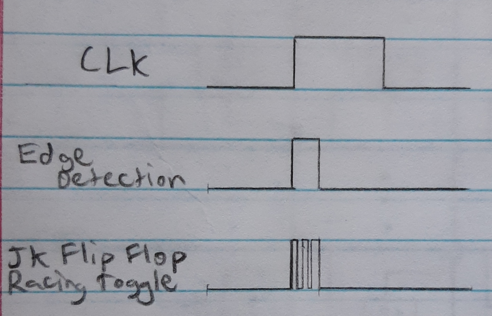
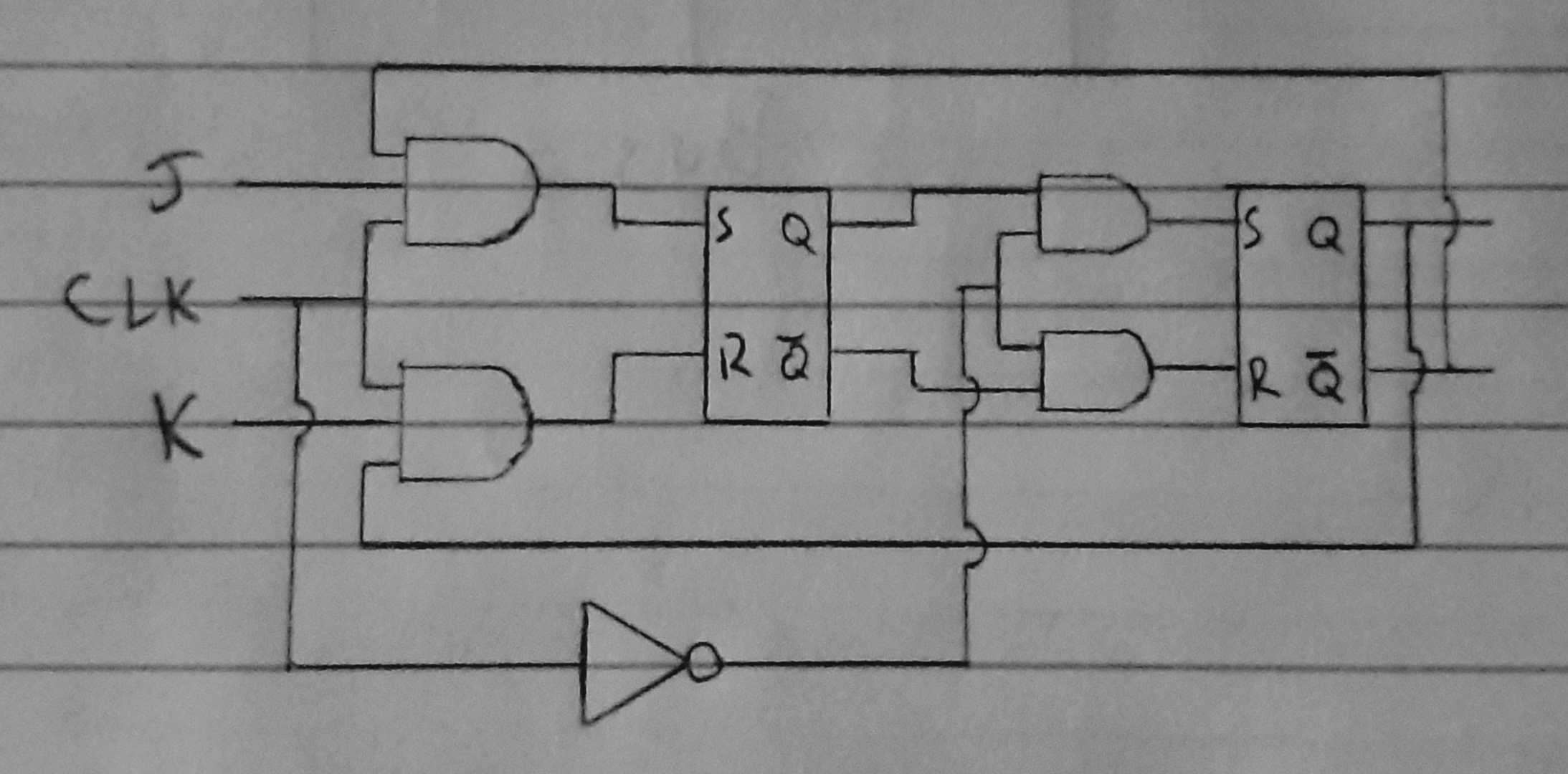
The Master Slave JK Flip Flop is used to solve this race condition problem with the toggle.
 |
 |
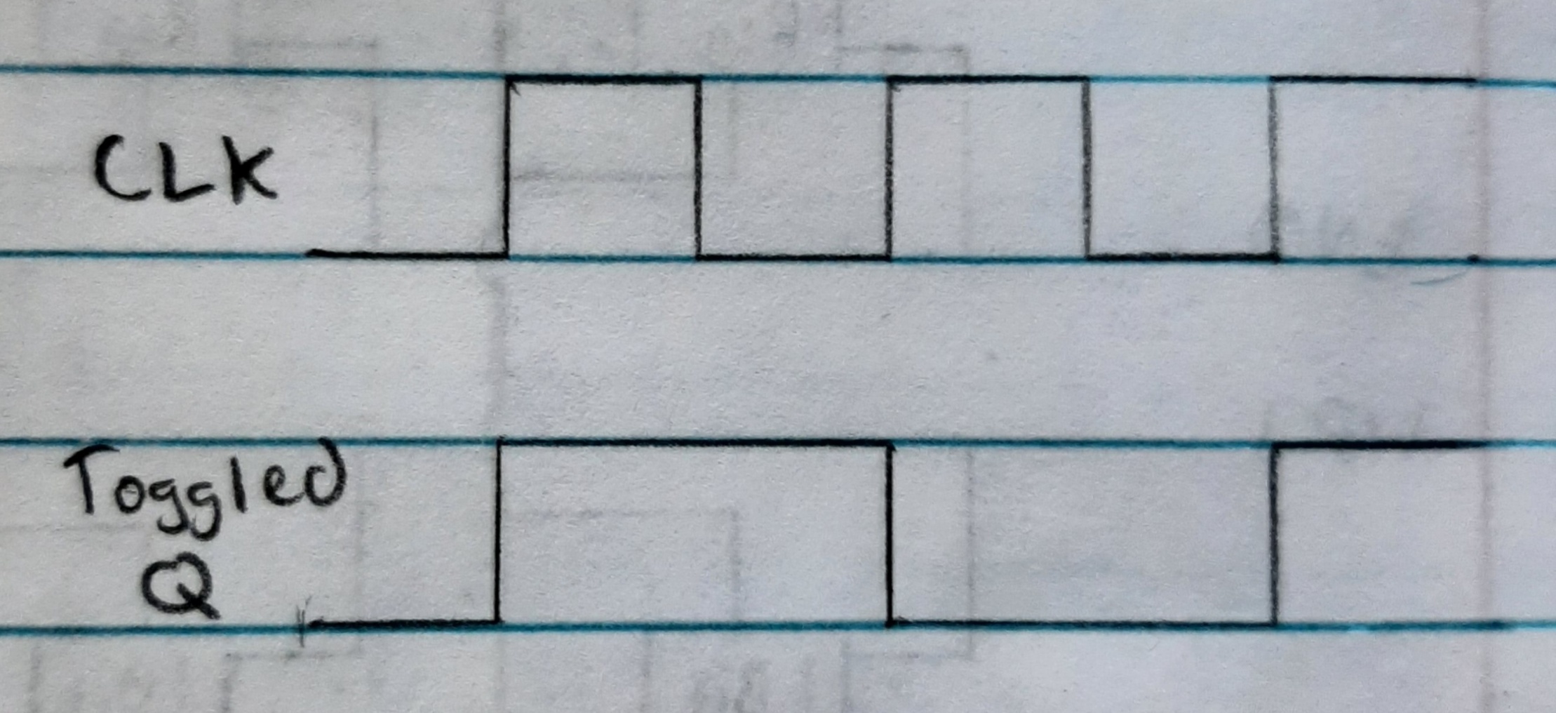
The binary counter is used to count 1, in binary, whenever the CLK goes from low to high.
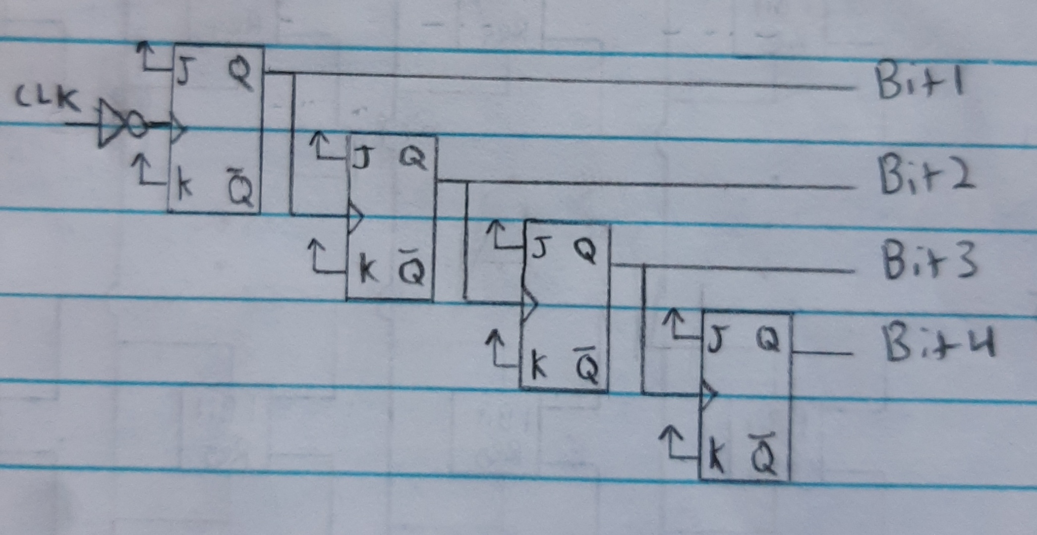
| Bit4 | Bit3 | Bit2 | Bit1 |
|---|---|---|---|
| $2^3$ | $2^2$ | $2^1$ | $2^0$ |
| 0 | 0 | 0 | 0 |
| 0 | 0 | 0 | 1 |
| 0 | 0 | 1 | 0 |
| 0 | 0 | 1 | 1 |
| 0 | 1 | 0 | 0 |
| etc | etc | etc | etc |
 |
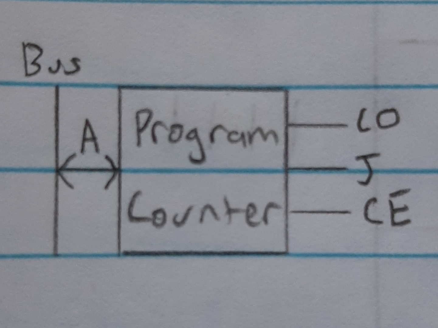 |
| Control Signal | Description |
|---|---|
| CO | Program Counter Out |
| CI/J | Program Counter In/Jump |
| CE | Count enable/Increment |
The control unit gets a CPU instruction, from the instruction register, and the step count, from the step counter, and outputs the correct control signals to execute that micro-instruction in the CPU.
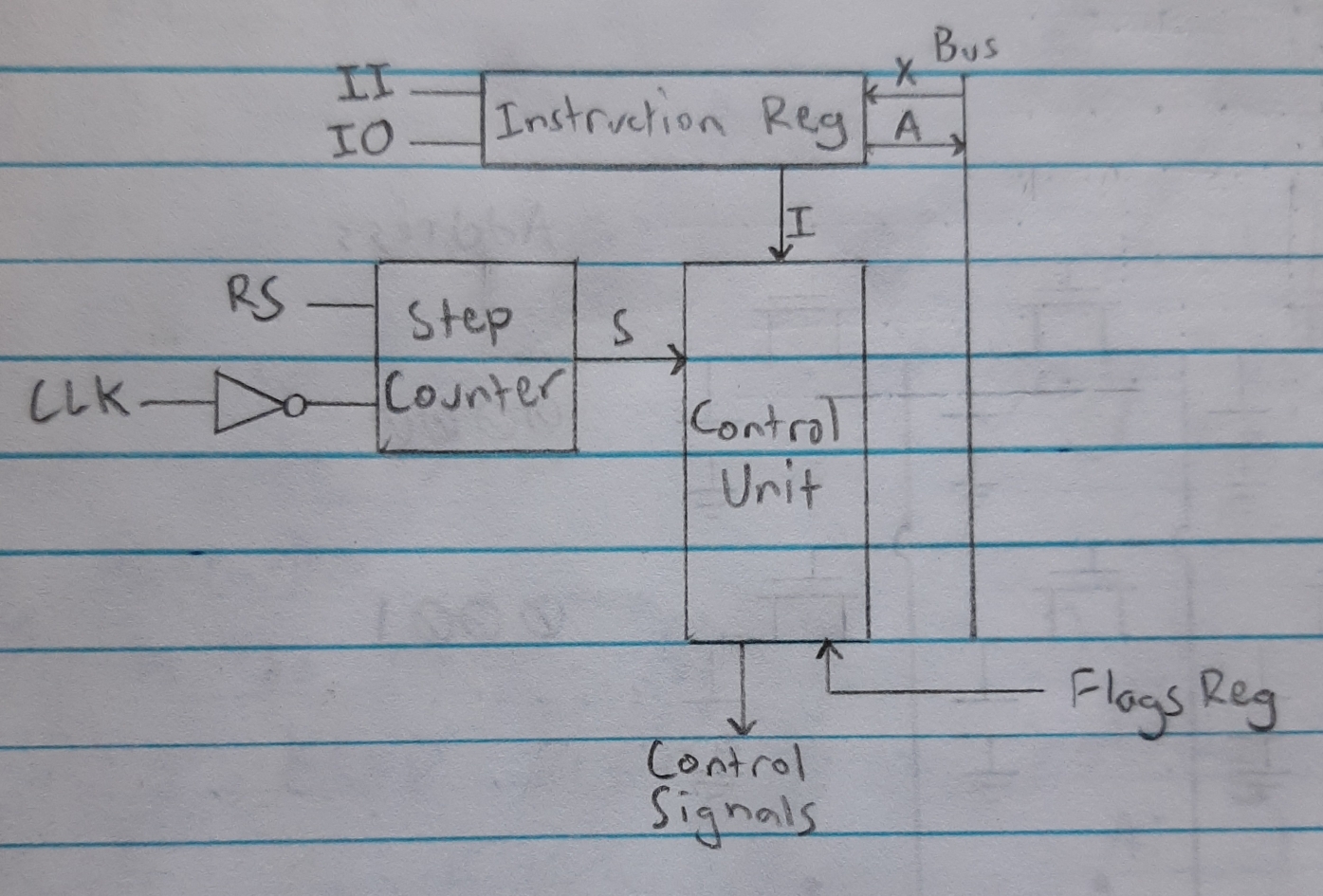
I symbolizes the amount of bits used to represent the instruction #. For this CPU, the instructions take up 4 bits.S symbolizes the number of bits used to represent how many steps are necessary to execute an instruction. This is usually 3 bits.The Fetch, Decode, and Execute are the steps that need to be taken in order to run code on the CPU. The code is stored in order in RAM. The program counter is used to store the current instruction that needs to be executed.
To make a CPU Turing complete, meaning it can compute any algorithm given enough time and memory, it must have a feedback mechanism. This mechanism involves checking the results of a computation and determining the next code to execute based upon those results. Conditional jumps allow for this feedback mechanism. They jump the program counter based upon the results of different flags.
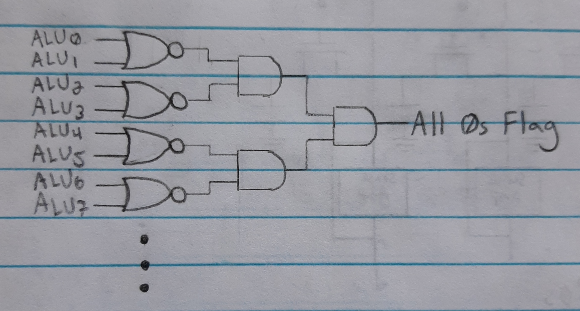
The flags need their own register to make sure they are saved before the calculation is put back in the A register.
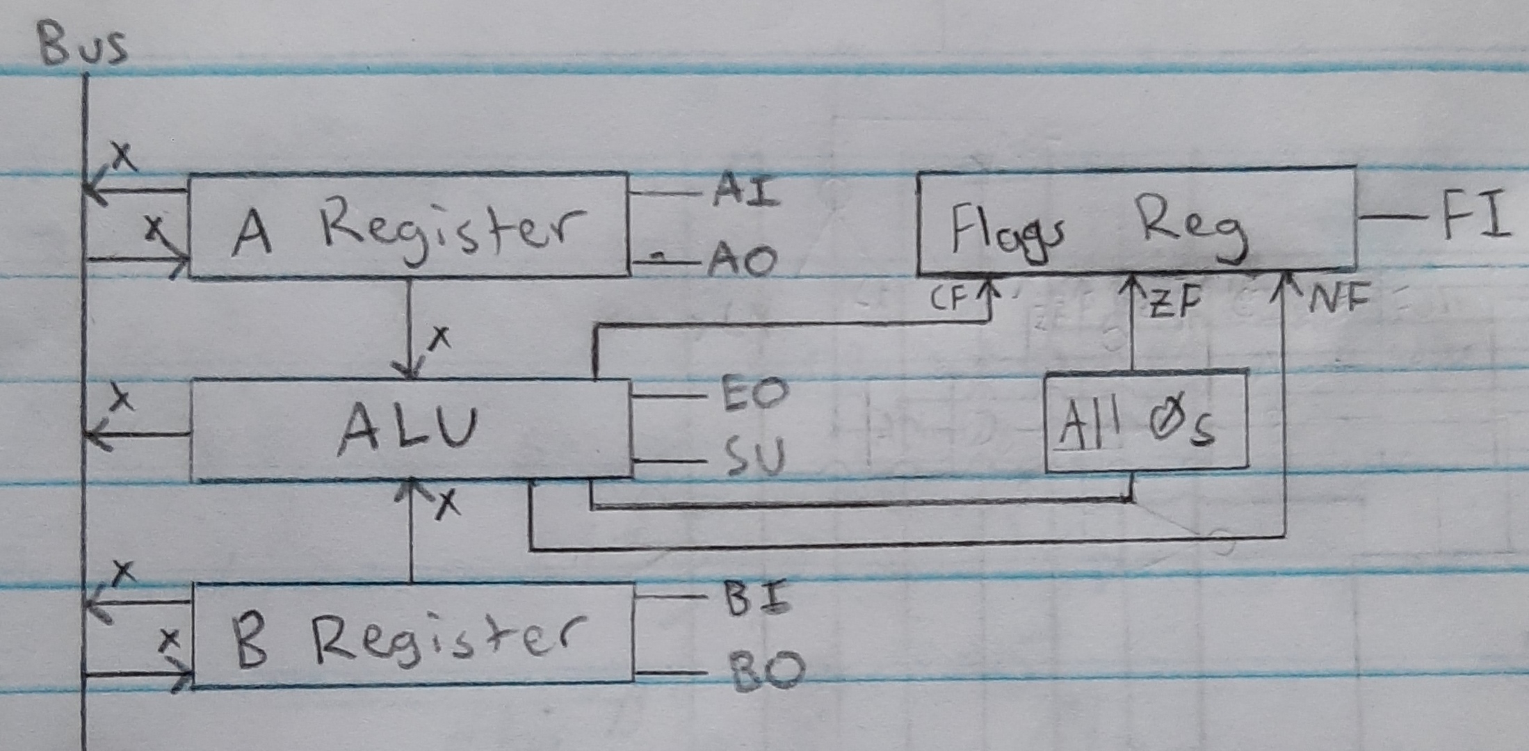
| Flag | Description |
|---|---|
| CF | Carry Flag |
| ZF | Zero Flag |
| NF | Negative Flag |
| Control Signal | Description |
|---|---|
| HT | Halt |
| MI | Memory Address In |
| RI | RAM In |
| RO | RAM Out |
| II | Instruction Register In |
| IO | Instruction Register Out |
| AI | A Register In |
| AO | A Register Out |
| EO | Sum Out |
| SU | Subtract |
| BI | B Register In |
| BO | B Register Out |
| OI | Output Register In |
| CE | Program Counter Enable/Increment |
| CO | Program Counter Out |
| CI | Program Counter In/Jump |
| UO | User Input Register In |
| FI | Flags Register In |
| RS | Reset Step Counter |
The instructions are programed into the Control Unit. They can be whatever the CPU designer wants them to be.
| Name | Instruction | Instruction # | Step Counter | CF | ZF | NF | Control Signal |
|---|---|---|---|---|---|---|---|
| Fetch | —- | 000 | - | - | - | CO, MI | |
| —- | 001 | - | - | - | RO, II, CE | ||
| No Operation | NOP | 0000 | 010 | - | - | - | |
| 011 | - | - | - | RS | |||
| Load A register | LDA Address | 0001 | 010 | - | - | - | IO, MI |
| 011 | - | - | - | RO, AI | |||
| 100 | - | - | - | RS | |||
| Add to A register | ADD Address | 0010 | 010 | - | - | - | IO, MI |
| 011 | - | - | - | RO, BI | |||
| 100 | - | - | - | EO, AI, FI | |||
| 101 | - | - | - | RS | |||
| Subtract from A register | SUB Address | 0011 | 010 | - | - | - | IO, MI |
| 011 | - | - | - | RO, BI | |||
| 100 | - | - | - | EO, AI, SU, FI | |||
| 101 | - | - | - | RS | |||
| Store A register in RAM | STA Address | 0100 | 010 | - | - | - | IO, MI |
| 011 | - | - | - | AO, RI | |||
| 100 | - | - | - | RS | |||
| Load Literal in A Register | LDL Literal | 0101 | 010 | - | - | - | IO, AI |
| 011 | - | - | - | RS | |||
| Jump Program Counter | JMP Address | 0110 | 010 | - | - | - | IO, CI |
| 011 | - | - | - | RS | |||
| Jump if Carry Flag | JC Address | 0111 | 010 | 1 | - | - | IO, CI |
| 010 | 0 | - | - | ||||
| 011 | - | - | - | RS | |||
| Jump if Not Carry Flag | JNC Address | 1000 | 010 | 0 | - | - | IO, CI |
| 010 | 1 | - | - | ||||
| 011 | - | - | - | RS | |||
| Jump if Zero/Equal | JZ/JE Address | 1001 | 010 | - | 1 | - | IO, CI |
| 010 | - | 0 | - | ||||
| 011 | - | - | - | RS | |||
| Jump if Not Zero/Not Equal | JNZ/JNE Address | 1010 | 010 | - | 0 | - | IO, CI |
| 010 | - | 1 | - | ||||
| 011 | - | - | - | RS | |||
| Jump if Negative | JN Address | 1011 | 010 | - | - | 1 | IO, CI |
| 010 | - | - | 0 | ||||
| 011 | - | - | - | RS | |||
| Jump if Positive | JP Address | 1100 | 010 | - | - | 0 | IO, CI |
| 010 | - | - | 1 | ||||
| 011 | - | - | - | RS | |||
| Compare A and B Register | CMP Address | 1101 | 010 | - | - | - | IO, MI |
| 011 | - | - | - | RO, BI | |||
| 100 | - | - | - | FI | |||
| 101 | - | - | - | RS | |||
| Output A Register | OUT | 1110 | 010 | - | - | - | AO, OI |
| 011 | - | - | - | RS | |||
| Halt CPU | HLT | 1111 | 010 | - | - | - | HT |
To get user input while the CPU is running, the user’s device can set an interrupt flag, which triggers the execution of code for handling user input. For example, if the user presses a key on the keyboard, the CPU receives an interrupt flag and executes the corresponding keyboard code. Once finished, it then continues from where it left off.
